What is a BJT or Bipolar Junction Transistor ?
What is a BJT?
A bipolar Junction transistor (BJT) is a three-terminal semiconductor device that consists of two p-n junctions. It is a current controlled device. The three terminals of the BJT are the Base, the Emitter and the Collector.
Construction of BJT
BJT is a semiconductor device that is constructed with Three doped semiconductor Regions. Base, Collector & Emitter separated by 2 p-n Junctions. Bipolar transistors are manufactured in two types, PNP and NPN, and are available as separate components, usually in large quantities. The prime use or function of this type of transistor is to amplify current. This makes them useful as switches or amplifiers. They have a wide application in electronic devices like mobile phones, televisions, radio transmitters, and industrial control.
Operation of BJT
There are three operating regions of a bipolar junction transistor:
- Active region: The region in which the transistors operate as an amplifier.
- Saturation region: The region in which the transistor is fully on and operates as a switch such that collector current is equal to the saturation current.
- Cut-off region: The region in which the transistor is fully off and collector current is equal to zero.
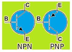
Types of BJT
There are two types of bipolar junction transistors:
- PNP bipolar junction transistor
- NPN bipolar junction transistor

Function of BJT
BJTs are of two types namely NPN and PNP based on doping types of the three main terminals. An NPN transistor consists of two semiconductor junctions that have a thin p-doped anode region and PNP transistor also consists of two SEMICONDUCTOR junctions that have a thin n- doped cathode region.
The flow of charge in a Bipolar transistor is due to the diffusion of charge carriers between the two regions belonging to different charge concentrations. Regions of BJT are known as the base, collector, and emitter. a
The emitter region is highly doped when compared to other layers. Both collector and base layers have the same charge carrier concentrations. Among these junctions, the base-emitter junction is forward biased, and the base-collector junction is reverse biased. Forward biased means p-doped region has more potential than the n-doped side.